- 您现在的位置:买卖IC网 > Sheet目录3880 > PIC16F785-I/SO (Microchip Technology)IC PIC MCU FLASH 2KX14 20SOIC
105
8272E–AVR–04/2013
ATmega164A/PA/324A/PA/644A/PA/1284/P
Note:
1. A special case occurs when OCR0A equals TOP and COM0A1 is set. In this case, the Com-
pare Match is ignored, but the set or clear is done at TOP. See ”Phase Correct PWM mode” on
page 101 for more details.
Bits 5:4 – COM0B1:0: Compare Match Output B mode
These bits control the Output Compare pin (OC0B) behavior. If one or both of the COM0B1:0
bits are set, the OC0B output overrides the normal port functionality of the I/O pin it is connected
to. However, note that the Data Direction Register (DDR) bit corresponding to the OC0B pin
must be set in order to enable the output driver.
When OC0B is connected to the pin, the function of the COM0B1:0 bits depends on the
WGM02:0 bit setting. Table 15-2 on page 104 shows the COM0A1:0 bit functionality when the
WGM02:0 bits are set to a normal or CTC mode (non-PWM).
Table 15-6 shows the COM0B1:0 bit functionality when the WGM02:0 bits are set to fast PWM
mode.
Note:
1. A special case occurs when OCR0B equals TOP and COM0B1 is set. In this case, the Com-
pare Match is ignored, but the set or clear is done atBOTTOM. See ”Fast PWM mode” on page
99 for more details.
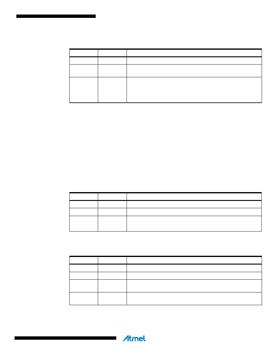
Table 15-4.
Compare Output mode, Phase Correct PWM mode
COM0A1
COM0A0
Description
0
Normal port operation, OC0A disconnected.
01
WGM02 = 0: Normal Port Operation, OC0A Disconnected.
WGM02 = 1: Toggle OC0A on Compare Match.
10
Clear OC0A on Compare Match when up-counting. Set OC0A on
Compare Match when down-counting.
11
Set OC0A on Compare Match when up-counting. Clear OC0A on
Compare Match when down-counting.
Table 15-5.
Compare Output mode, non-PWM mode.
COM0B1
COM0B0
Description
0
Normal port operation, OC0B disconnected.
0
1
Toggle OC0B on Compare Match
1
0
Clear OC0B on Compare Match
1
Set OC0B on Compare Match
Table 15-6.
Compare Output mode, Fast PWM mode (1).
COM0B1
COM0B0
Description
0
Normal port operation, OC0B disconnected.
01
Reserved
10
Clear OC0B on Compare Match, set OC0B at BOTTOM,
(non-inverting mode).
11
Set OC0B on Compare Match, clear OC0B at BOTTOM,
(inverting mode).
发布紧急采购,3分钟左右您将得到回复。
相关PDF资料
PIC16C56A-04/SO
IC MCU OTP 1KX12 18SOIC
PIC18F23K20-I/MV
IC MCU 8BIT 8KB FLASH 28UQFN
PIC16F627A-I/P
IC MCU FLASH 1KX14 EEPROM 18DIP
XF2G-1414-11
CONN FPC 14POS 0.5MM SMT
PIC16F777T-I/ML
IC PIC MCU FLASH 8KX14 44QFN
PIC18F2539T-E/SO
IC PIC MCU FLASH 12KX16 28SOIC
PIC16LF1936-I/SO
IC PIC MCU FLASH 512KX14 28-SOIC
PIC16F873AT-E/ML
IC PIC MCU FLASH 4KX14 28QFN
相关代理商/技术参数
PIC16F785-I/SS
功能描述:8位微控制器 -MCU 3.5KB FL 128R 18 I/O RoHS:否 制造商:Silicon Labs 核心:8051 处理器系列:C8051F39x 数据总线宽度:8 bit 最大时钟频率:50 MHz 程序存储器大小:16 KB 数据 RAM 大小:1 KB 片上 ADC:Yes 工作电源电压:1.8 V to 3.6 V 工作温度范围:- 40 C to + 105 C 封装 / 箱体:QFN-20 安装风格:SMD/SMT
PIC16F785T-E/SS
功能描述:8位微控制器 -MCU 3.5KB FL 128R 18 I/O RoHS:否 制造商:Silicon Labs 核心:8051 处理器系列:C8051F39x 数据总线宽度:8 bit 最大时钟频率:50 MHz 程序存储器大小:16 KB 数据 RAM 大小:1 KB 片上 ADC:Yes 工作电源电压:1.8 V to 3.6 V 工作温度范围:- 40 C to + 105 C 封装 / 箱体:QFN-20 安装风格:SMD/SMT
PIC16F785T-I/ML
功能描述:8位微控制器 -MCU 3.5 KB 128 RAM 18I/O RoHS:否 制造商:Silicon Labs 核心:8051 处理器系列:C8051F39x 数据总线宽度:8 bit 最大时钟频率:50 MHz 程序存储器大小:16 KB 数据 RAM 大小:1 KB 片上 ADC:Yes 工作电源电压:1.8 V to 3.6 V 工作温度范围:- 40 C to + 105 C 封装 / 箱体:QFN-20 安装风格:SMD/SMT
PIC16F785T-I/ML036
制造商:Microchip Technology Inc 功能描述:
PIC16F785T-I/ML045
制造商:Microchip Technology Inc 功能描述:
PIC16F785T-I/SO
功能描述:8位微控制器 -MCU 3.5KB FL 128R 18 I/O RoHS:否 制造商:Silicon Labs 核心:8051 处理器系列:C8051F39x 数据总线宽度:8 bit 最大时钟频率:50 MHz 程序存储器大小:16 KB 数据 RAM 大小:1 KB 片上 ADC:Yes 工作电源电压:1.8 V to 3.6 V 工作温度范围:- 40 C to + 105 C 封装 / 箱体:QFN-20 安装风格:SMD/SMT
PIC16F785T-I/SS
功能描述:8位微控制器 -MCU 3.5KB FL 128R 18 I/O RoHS:否 制造商:Silicon Labs 核心:8051 处理器系列:C8051F39x 数据总线宽度:8 bit 最大时钟频率:50 MHz 程序存储器大小:16 KB 数据 RAM 大小:1 KB 片上 ADC:Yes 工作电源电压:1.8 V to 3.6 V 工作温度范围:- 40 C to + 105 C 封装 / 箱体:QFN-20 安装风格:SMD/SMT
PIC16F818-E/ML
功能描述:8位微控制器 -MCU 1.75KB 128RAM 16 I/O Ext Temp QFN28 RoHS:否 制造商:Silicon Labs 核心:8051 处理器系列:C8051F39x 数据总线宽度:8 bit 最大时钟频率:50 MHz 程序存储器大小:16 KB 数据 RAM 大小:1 KB 片上 ADC:Yes 工作电源电压:1.8 V to 3.6 V 工作温度范围:- 40 C to + 105 C 封装 / 箱体:QFN-20 安装风格:SMD/SMT